1B21
Rev. C | Page 5 of 8
INSIDE THE 1B21
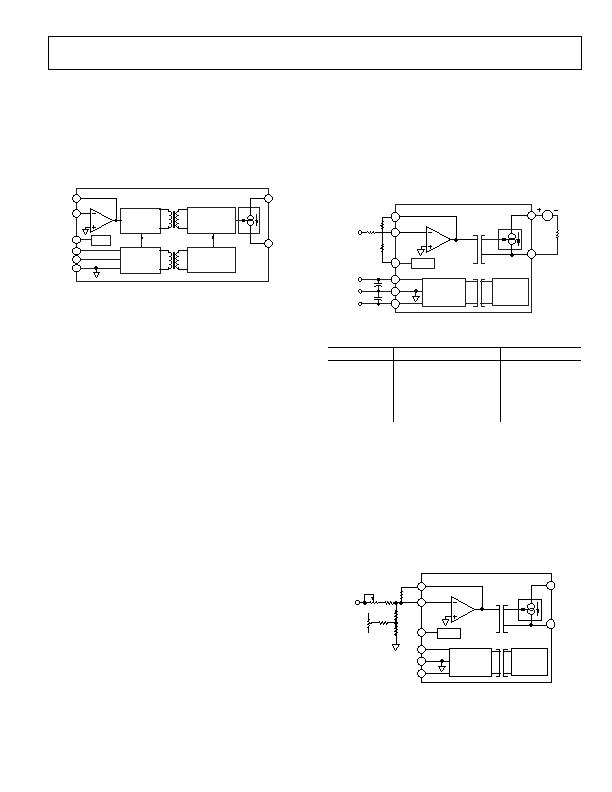
Referring to the functional block diagram (see Figure 3), the
?5 V power inputs provide power to both the input side
circuitry and the power oscillator. The 25 kHz power oscillator
provides both the timing information for the signal modulator
and drives transformer T2 for the output side power supplies.
The secondary winding of T2 is full wave rectified and filtered
to create the output side power.
This maps the input voltage into a 4 V span. To create a 1 V
offset at the output of the internal amplifier (4 mA at the output
of the 1B21) a current derived from the reference can be fed
into the summing node. The offset resistor (for a 1 V output
offset) is given by the equation: RO = 6.225 RF. For most
applications, it is recommended that RF be in the 25 k??0%
range. Resistor values for typical input and output ranges are
shown in Table 2.
18
1
38
17
19
20
22
21
COM
T2
1B21
FB
INPUT
OUT
HIGH
OUT
LOW
REF
OUT
+15V
15V
T1
SIGNAL
ISOLATION
POWER
ISOLATION
TIMING
TIMING
RECTIFIER
OSCILLATOR
MODULATOR
DEMODULATOR
REF
LOOP
Figure 3. 1B21 Functional Block Diagram
The input stage is configured as an inverting amplifier with
three user-supplied resistors for gain, offset, and feedback.
The conditioned signal is modulated to generate a square wave
with a peak-to-peak amplitude proportional to VIN. The signal
drives the signal transformer T1. An internal reference with a
nominal output voltage of +6.225 V and tempco of ?5 ppm/癈
is provided to develop a 4 mA offset for 4 mA to 20 mA current
loop applications.
After passing through signal transformer T1, the amplitude
modulated signal is demodulated and filtered by a single pole
filter. Timing information for the output side is derived from
the power transformer T2. The filtered output provides the
control signal for the voltage-to-current converter stage. An
external power supply is required in series with the load to
complete the current loop.
USING THE 1B21
Input Configurations
The 1B21 has been designed with a flexible input stage for a
variety of input and output ranges. The basic interconnection
for setting gain and offset is shown in Figure 4. The output of
the internal amplifier is constrained to 0 to 5 V, which maps
into 0 to 20 mA across the isolation barrier. Thus to create a
4 mA offset at the output, the input amplifier has to be offset
by 1 V.
For example, for 0 to 20 mA operation, the transfer function for
the input stage is
5/V
IN
= R
F
/R
I
and no offset resistor is needed. For 4 mA to 20 mA operation
one gets
4/VIN = RF/RI
1
38
RECTIFIER
OSCILLATOR
REF
V
IN
+15V
COM
15V
R
I
R
LOAD
R
F
R
O
18
17
19
20
4.7礔/20V
+
+
22
21
FB
INPUT
1B21
Figure 4. Basic Interconnections
Table 2. Resistor Values for Typical Ranges
Input Volts Output mA RI k? RF k? RO k?
0 to 5
0-20
25 25 Open
0 to 10
0-20
50 25 Open
0 to 5
4-20
25 20 124.3
0 to 10
4-20
50 20 124.3
1 to 5
4-20
25 25 Open
Adjustments
Figure 5 is an example of using potentiometers for trimming
gain and offset for a 0 V to 5 V input and 0 V to 20 mA output.
The network for offset adjustment keeps the resistors relatively
small to minimize noise effects while giving a sensitivity of ?%
of span. For more adjustment range, resistors smaller than 274 k
can be used. Resistor values from Table 2 can be substituted for
other input and output ranges.
In general, any bipolar voltage can be input to the 1B21 as
long as it is offset to meet the 0 V to 5 V constraint of the
modulator and the input signal range is 1 V minimum.
1
38
RECTIFIER
OSCILLATOR
REF
V
IN
+15V
COM
15V
18
17
1k&
50k&
19.6k&
20k&
FB
INPUT
20k&
274k&
19
20
21
22
1k&
+15V
15V
1B21
Figure 5. Offset and Span Adjustment
发布紧急采购,3分钟左右您将得到回复。
相关PDF资料
1B22AN
IC VOLTAGE CONVERTER PROG DIP
AD536AKQ
IC TRUE RMS/DC CONV 14CDIP
AD537SD
IC V/F CONV 14-CDIP
AD636JD
IC TRUE RMS/DC CONV MONO 14-CDIP
AD650SD
IC V-F/F-V CONV 1MHZ 14-CDIP
AD652SQ
IC V-F CONV SYNCH MONO 5V 16CDIP
AD654JNZ/+
IC CONV VOLT-FREQ 500KHZ 8DIP
AD7740YRM
IC CONVERTER V TO FREQ 8-MSOP
相关代理商/技术参数
1B21-N2F4H9AE
制造商:Eledis 功能描述:
1B21-NF1PCSE
制造商:Alpha 3 Manufacturing 功能描述:
1B21-NF1STAE
制造商:Alpha 3 Manufacturing 功能描述:
1B21-NF1STAE-Z
制造商:Alpha 3 Manufacturing 功能描述: 制造商:Eledis 功能描述:
1B21-NF4H9AE
制造商:Alpha 3 Manufacturing 功能描述: 制造商:ELEDIS 功能描述:DPDT.WASH TOGG
1B21-NF4H9SE
制造商:Alpha 3 Manufacturing 功能描述:
1B21-NF4U2SAE-DWG1154
制造商:Alpha 3 Manufacturing 功能描述:
1B22
制造商:AD 制造商全称:Analog Devices 功能描述:Programmable, Isolated Voltage-to-Current Converter